Solar cell manufacturing has evolved significantly in recent years. As solar energy is predicted to experience extraordinary growth, the near future will likely be marked by even more technological innovations.
In this article, we’ll cover the steps of the solar cell manufacturing process. We’ll also highlight challenges and advancements to make solar photovoltaic cells more efficient and sustainable.
The process of turning raw materials into high-performance photovoltaic cells is intricate. Fundamentally, the technique uses the photovoltaic effect—in which photons excite electrons in a semiconductor material to produce an electric current—to transform sunlight into solar energy. Here are the 5 main steps:
From raw materials to ingots: The manufacturing process begins with polysilicon, a purified form of metallurgical-grade silicon extracted from quartz sand using the floating zone method (FZ). This pure silicon is then melted and formed into either monocrystalline silicon or polycrystalline silicon ingots, thanks to the Czochralski (CZ) process.
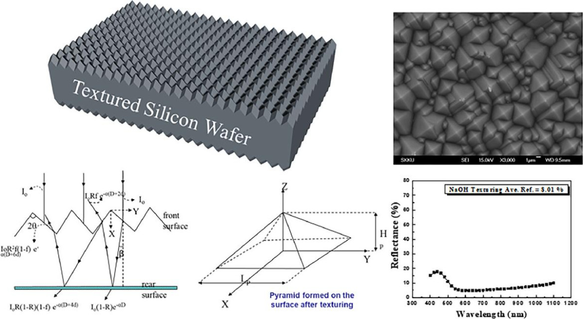
From ingots to wafers: Next, the silicon ingots are sliced into thin silicon wafers. These wafers serve as the foundation for solar cells. The most common solar panels and PV modules are made with hexagonal or rectangular cells. The silicon wafer disks are then cleaned and textured to minimize sunlight reflection losses.
Wafer doping: After being cleaned and treated, the wafers undergo doping—a process in which layers of transparent conductive oxides and dopants like boron and phosphorus are introduced to make the wafers electrically conductive. This step is also called the diffusion process. At this point, an electrical path is established between the front and rear of the wafer. This path is eliminated around the wafer edge during the edge isolation procedure (using laser edge deletion or plasma etching) to prevent short circuits and improve durability.
Wafer coating: The wafers are then coated with silicon nitride or titanium oxide, an anti-reflective material that improves light absorption and decreases reflection. The most common method for depositing anti-reflective coating on the wafer is Plasma Enhanced Chemical Vapor Deposition(PECVD).
Contact Printing: The final step consists of screen printing metal contacts on the wafer to collect and transmit electricity through ohmic contact. These contacts are generally made of silver or copper paste. The screen-printed wafers then go through a sintering furnace to solidify the metal contacts before being cooled.
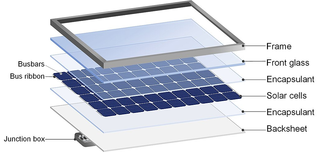
Solar panels are then created by joining the solar cells into modules, encasing them in layers of ethylene vinyl acetate (EVA), and adding a glass cover and back sheet for durability.
To make electrical connections easier, photovoltaic modules come with a junction box. The direct current (DC) electricity produced by the cells is transformed into alternating current (AC) electricity by an inverter that is fixed to the solar panel.
The image below shows the multiple components used in assembling solar modules.
Despite a rapid decrease in manufacturing costs, clean energy obtained from solar panels still faces various efficiency and sustainability challenges. However, key advancements in materials and manufacturing techniques promise exciting developments.
Here are today’s most important innovations.
Improved Technology
The solar industry is used to produce solar cells that absorb light on one side. Recent innovations have allowed the increased production of bi-facial modules, allowing light absorption on both sides of the solar module.
Passivated Emitter and Rear Contact (PERC) solar cells are also gaining popularity in solar panel production. These upgraded cells produce up to 12% more energy, thanks to an extra layer placed on the cell’s rear side that reflects sunlight back into the solar cell.
Looking forward, TOPCon and Heterojunction (HJT) solar devices are expected to become the main types of solar cells being manufactured. Besides having a low integration cost to existing lines, they allow many of the per-square-meter efficiency gains inherited from previous innovations, resulting in a more economical system.
Alternative Materials
Alternative materials have recently gained more attention within the industry. For example, thin-film cadmium telluride (CdTe) and Perovskite solar cells (PSC) have a wider wavelength absorption capacity and offer relatively high efficiency rates compared to traditional crystalline silicon cells.
Also, PSCs are compatible with curved and flexible surfaces and are generally much thinner than crystalline silicon cells, which creates new possibilities for solar technology.
However, perovskite degrades much faster than silicon. For this reason, perovskite and crystalline silicon hybrid (multi-junction) technologies are becoming more popular because they increase energy output while remaining affordable.
These multi-junction cells can typically boost efficiency for the first 10 to 15 years and then offer the normal efficiency of a traditional silicon cell. Thanks to the combined materials, multi-junction cells absorb a much wider range of the light spectrum.
Increased Sustainability
A growing number of manufacturers have adopted green solvents or solvent-free material treatment processes. The integration of laser technology into production lines also helps reduce waste, material consumption and cycle times significantly.
The improved efficiency and lifetime of solar cells also contribute to reducing waste and raw material consumption. Companies like First Solar have implemented recycling programs that recover up to 95% of semiconductor materials and 90% of glass from decommissioned modules.
Establishing circular water strategies in solar cell production facilities can also reduce water consumption by up to 79%.
Laser technology can play an important role in enhancing the efficiency and manufacturing process sustainability of solar cells, solar modules, and solar panels.
This process removes conductive coatings from thin-film solar cells to prevent short circuits, ensuring the reliability and longevity of the panels by leaving a clean glass surface.
This sustainable method offered by Laserax ensures minimum substrate damage and high throughput consistency.
Thin-Film Cleaning for Recycling
By providing a precise and contact-free method for cleaning surfaces, laser cleaning systems enhance adhesion quality for coatings and encapsulants, improving the performance of solar modules.
Laserax’s laser-based material removal technique allows solar panel manufacturers to separate the coatings and recover valuable materials with high precision.
Laser Welding for Interconnections
A high-speed, non-contact laser welding system can create precise welds between solar cell components (e.g. tabs, busbars) and enhance production efficiency. Laser welding is typically 10 times faster than traditional ultrasonic bonding, making the process more scalable.
Laser Wafer Dicing
Wafer dicing consists of separating individual chips in a semiconductor wafer. Laser marking can be an ideal option for wafer dicing because of its high speed, damage-free and consumable-free process.
Ingot and Component Marking
The silicon ingots used to produce wafers require etching for optimal cutting and wafer traceability. Ensuring traceability of solar cell components is vital for quality control and regulatory compliance.
Laser marking systems that do not affect cell performance can achieve precise, contact-free and treatment-resistant marking on solar cell components.
Laserax plays a crucial role in advancing solar cell manufacturing by offering specialized laser solutions that improve efficiency, quality, and sustainability.
Contact us to discuss your application with an expert.
Dr. Annick Anctil is an Associate Professor at the Michigan State University’s College of Engineering, where she leads research on anticipatory sustainability assessment. She uses proactive sustainability assessment to reduce the environmental and cost impact of new technologies. The core of her research is evaluating the environmental impact of photovoltaics and battery technologies, particularly the effect of mining and recycling materials for energy applications.
Laserax manufactures OEM laser systems and turnkey laser machines to easily integrate laser marking, laser cleaning, laser texturing and laser hardening in production lines. Providing laser expertise, its solutions are safe and efficient.
Solar energy is booming, and solar panel manufacturing is at the heart of this revolution. In this article, we’ll explore how solar panels are made and the biggest challenges faced within the solar energy supply chain. We’ll also cover recent improvements and opportunities to overcome these challenges, including laser technology.


