Every printed circuit board that leaves a fabrication line needs to be traceable to its source.
Traceability data (serial numbers, lot codes, Data Matrix symbols) must survive assembly, reflow, cleaning, coating, and years of field service, all while fitting within a marking area smaller than a grain of rice.
That combination of permanence and precision is why laser marking has become the standard method for identifying PCBs.
The challenge is that a PCB is not a forgiving surface. Solder masks, laminates, exposed copper, and nearby components are all sensitive to heat and energy in different ways. A marking process that produces crisp, high-contrast codes on one board can char, discolor, or damage the next.
So, choosing the right laser marking machine is critical.
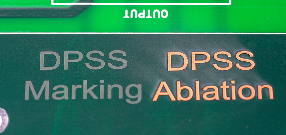
PCB laser marking uses a focused laser beam to create a permanent, machine-readable mark directly on a printed circuit board, eliminating the need for ink, adhesive labels, or physical contact with the part.
Rather than printing or applying something to the board, the laser interacts with the material itself to produce a mark that becomes part of the component.
That mark can be placed in several locations on a board, depending on the product and traceability strategy:
Solder masks
Exposed FR-4 laminate
Exposed copper or other conductive layers
Flexible and ceramic substrates
Discrete electronic components
Metal shields or enclosures
The content of the mark varies by application and might include Data Matrix codes, QR codes, sequential serial and lot numbers, and logos or certification marks required for regulatory or brand purposes.
Why Use Laser Marking for PCB Identification?
Laser marking has largely replaced labels and ink-based printing on PCBs because it produces a mark that lasts as long as the board does without adding materials, consumables, or manual steps to the process.
Permanent Traceability
A laser-marked code becomes part of the board's surface rather than something attached to it, so it can follow a unit from fabrication through assembly, testing, installation, and field servicing without falling off or wearing away. This is especially important in the automotive, aerospace, and medical device industries, where a board's history must remain traceable for years.
Small, High-Resolution Codes
Laser systems can produce extremely fine, high-resolution marks, letting manufacturers fit a fully machine-readable identifier into a marking area only a millimeter or two across. This allows serialization at both the board level and the individual component level.
No Inks or Labels
Because the laser marks the material directly, there's nothing to run out of, order, or store. Manufacturers eliminate label rolls, ink cartridges, and related inventory management, along with the risk of adhesive contamination or a label peeling off during handling, reflow, or cleaning.
Contactless Process
Laser marking never touches the part, so there's no risk of mechanical damage from a stamping or engraving tool, and no risk of electrostatic discharge from human handling during marking.
Production-Line Automation
Laser marking systems integrate naturally into automated lines. They can generate unique identifiers on the fly from a connected database, and can read and verify each code immediately after marking, thereby closing the loop on track-and-trace without a separate inspection.
Comparing Laser Marking vs. Labels or Inkjet Printing
Another reason manufacturers choose laser marking is because of how it stacks up against labels or inkjet printing. Here’s how these options compare.
Laser Marking
Labels
Injet Printing
Permanence
Becomes part of the board, survives reflow, cleaning, and field life
Can peel, fade, or detach over time
Can smear or wear, especially with solvent exposure
Resolution
Very high, supports fine Data Matrix and QR codes
Limited by print resolution and label size
Moderate, depending on the droplet size
Consumables
None
Labels, adhesive stock
Ink, cartridges
Automation Fit
Integrates with vision and code verification
Requires label applicators
Requires nozzle maintenance
Risk of Detachment
None, mark is part of the substrate
High
Low, but surface adhesion can fail
Which Laser Type Is Best for PCB Marking?
The right choice of laser technology depends on the PCB substrate, the solder-mask color and formulation, and the size of the code being marked.
UV Lasers
UV lasers are usually the leading choice for FR-4, solder masks, sensitive plastics, and miniature codes. Their short wavelength allows for a very small spot size and a limited heat-affected zone, producing fine, legible marks without the surrounding thermal damage that larger, hotter beams can cause.
Results still depend on the specific board material and solder-mask formulation and color. As a general rule, darker solder masks produce better contrast under laser marking than very light or bright ones.
UV is a good choice when testing confirms that the mark remains readable after reflow, cleaning, coating, abrasion, and environmental exposure.
Fiber Lasers
Fiber lasers are best suited to exposed metals, shields, housings, and engineered plastics compatible with their higher energy density, and are a strong fit when a small spot size isn't the priority or the material isn't heat-sensitive. On many PCB laminates, however, fiber lasers produce more thermal effect than the material can tolerate.
CO2 Lasers
CO2 lasers work well on certain organic materials and coating-removal applications, but run hotter than the other two options. If heat isn't a major concern and the area to be marked is relatively large, a CO2 laser can be a cost-effective choice.
CO2 spot size is 10x larger than fiber lasers and 30x large then UV, so they are more suitable for larger marks. A greater thermal impact also limits effectiveness for very small PCB codes of tightly packed marks.
Why Sample Testing Is Essential
Material response varies between suppliers, coating batches, and solder-mask colors. The only reliable way to select a laser is to test every substrate, color, coating, and supplier variation that will actually appear in production.
Key Features to Look for in a PCB Laser Marking Machine
Appropriate Wavelength and Pulse Characteristics
The laser's energy absorption and pulse duration need to match the PCB material and the type of mark being created, whether that’s a surface color change or a deeper ablation mark. Getting this right means balancing contrast, surface alteration, spot size, and thermal exposure.
Spot Size and Beam Quality
Spot size determines the minimum code dimensions and how sharp the edges of each mark element are. Don’t rely on resolution specs alone, you need readable codes that work for both the human eye and vision systems.
Power Matched to Cycle Time
More wattage is not automatically better. The right power level should be evaluated using an actual production code, material, and takt time.
Field of View and Working Distance
The system needs to cover the entire board or panel area that requires marking. There's a real trade-off here: a larger field of view generally comes at some cost to marking resolution, so this should be sized to the actual board layout rather than maximized by default.
Vision, Fiducial Recognition, and Autofocus
Boards rarely arrive in a perfectly consistent position. Vision systems, fiducial recognition, and autofocus let the machine locate each board despite positional variation, align marks against PCB fiducials, and compensate for height differences or warpage to prevent marks from landing in the wrong location.
Integrated Code Reading and Verification
A marking machine should confirm, immediately after marking, that every identifier is present and readable. This also catches duplicate, incomplete, or incorrectly positioned codes, and records verification results as part of the board's traceability record.
Serialization and Factory Connectivity
The machine should communicate with PLCs, MES, ERP systems, or traceability databases, generate unique codes automatically, and associate each marking result with the corresponding production record.
PCB Handling and Automation
Depending on volume, the system may need to support panel conveyors, SMEMA-compatible equipment, custom fixtures, or robotic handling. Worth consideration are automatic width adjustment, board clamping, and bypass modes.
ESD Control, Fume Extraction, and Laser Safety
Electronic assemblies need protection from electrostatic discharge throughout marking, and the process itself can generate particles and fumes that need to be captured. Where practical, an enclosed Class 1 laser system is preferable, since it removes the need for additional operator safety controls.
Choose the Right Machine Configuration
You should choose a machine configuration based on your production volume, loading method, board variability, and integration requirements.
Enclosed Workstation
Best for: Prototyping, laboratory work, repair operations, and low-to medium-volume production.
Evaluate manual loading, fixture design, and operator ergonomics, since a person is typically involved in every cycle.
Inline Laser Marking System
Best for: High-volume PCB fabrication or assembly, integrated directly into the production line.
Evaluate conveyor integration, cycle time, automatic code verification, and how well the system communicates with the rest of the line.
Flexible Precision or Robotic System
Best for: Lines handling multiple board formats, variable marking positions, or complex assemblies, where a fixed configuration can't offer enough adaptability.
Evaluate changeover time and the programming effort required each time the setup changes.
How to Validate a PCB Laser Marking Machine Before Purchasing
Before approving a machine, test it under conditions that reflect daily production.
Use actual production boards rather than generic test coupons. Include every relevant solder-mask color, substrate, coating, and supplier to identify variations that could affect marking results.
Verify code quality immediately after marking and again after reflow, cleaning, coating, and handling. Check for discoloration, delamination, carbonization, exposed conductors, and any change in electrical performance.
Measure the complete cycle, including board positioning, marking, code verification, and data exchange. This determines whether the machine can meet the line’s actual takt time and reveals potential bottlenecks.
Common PCB Laser Marking Mistakes
A number of avoidable mistakes show up repeatedly when manufacturers evaluate or implement PCB laser marking, such as:
Selecting the laser based on wattage alone, rather than on how it performs on the actual material and code.
Testing a single solder-mask color and assuming other colors or supplier variants will behave the same way.
Evaluating how a mark looks without verifying that it actually scans reliably.
Ignoring PCB warpage and the positional tolerances that come with real production boards.
Measuring only laser exposure time instead of the full production cycle.
Failing to test how a mark holds up after downstream processes like reflow or coating.
Treating software and traceability integration as an afterthought instead of a core requirement.
Frequently Asked Questions
Can laser marking damage a PCB?
If the wrong laser or wrong parameters are used, marking can damage a board. In extreme cases, incorrect settings can cut into the PCB rather than mark its surface.
Is a UV laser always the best choice for PCB marking?
UV lasers offer the most flexibility, the smallest spot sizes, and the least heat, which makes them a strong default. They are, however, more expensive than fiber or CO2 lasers, so the right choice still depends on the application.
Should PCBs be marked before or after assembly?
This is largely a customer choice that depends on the facility's setup and whether the mark is used internally or needs to be visible to the end user.
How small can a laser-marked Data Matrix code be?
With a UV laser capable of a 10-micron cell size, it's possible to achieve a 120-by-120-micron Data Matrix code using a 12-by-12 cell grid.
Can a laser mark through coatings?
Yes, depending on the coating. The coating must be transmissive to the wavelength of the laser being used.
Does a PCB laser marking machine need an integrated vision system?
Not necessarily. It depends on the customer's existing tooling and the level of accuracy required for the application.
Are You Looking for a Laser Marking Machine for PCBs?
Send Laserax a set of representative PCBs, and our team can run application testing and provide configuration recommendations tailored to your boards, materials, and production requirements.
Alex Laymon became President and Director of DPSS Lasers (now a Laserax company) in 1998. He previously served as the Vice President of Engineering at LiCONiX, following a series of technical positions that included Engineering Manager and Senior Laser Engineer. Mr. Laymon received his B.S. in Engineering Physics and his M.B.A. at Santa Clara University. His decades of expertise in UV lasers now contribute to Laserax's mission to shape the future of high-precision laser solutions.
Semiconductor manufacturing requires incredible precision. In an industry where one micron is considered large, even minor process deviations can compromise yield or performance. Laser wafer marking is often the best solution, offering non-contact processing with high repeatability and integration into automated workflows.
When precision marking is required on delicate or heat-sensitive materials, ultraviolet (UV) laser technology offers a distinct advantage.
By minimizing thermal impact, UV laser marking creates high-contrast, permanent marks while preserving material integrity and meeting demanding traceability requirements.
Walk into any Hospital and you'll see it immediately. Every single tool, implant, and device has some kind of marking on it. Serial numbers, logos, barcodes. When you're putting something inside someone's body, or even just touching their skin, you need to know exactly what it is, where it came from, and when it was made.